Research highlights from Fraunhofer IZM-ASSID

© Fraunhofer IZM-ASSID
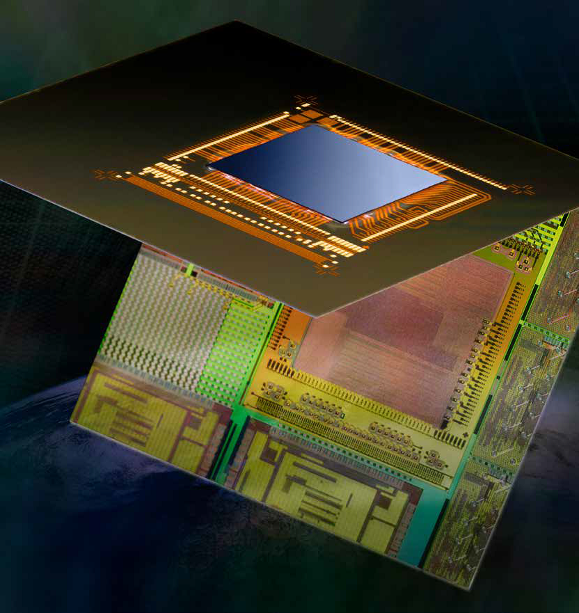
Security-Demonstrator mit 3D-integriertem Security-Controller mit Nah-Feld-Kommunikations- Chip (NXP). Auf der Oberseite sind die zusätzlichen neu entwickelten und validierten 3D-Teststrukturen sichtbar, welche ein erweitertes 3D-Prozessmonitoring erlauben.

3D process technology for innovative system in package (3D-SiP) solutions

The integration density of active components is a key factor in the development of new products. But technical boundaries and rising costs are limiting the structure size reduction. A three-dimensional stacking of chips, combined with wafer level processing, allows a functional extension and an increased complexity of electronic systems within minimum space.

The European joint project Master_3D aimed at the establishment of an integrated platform (tools, materials, processes) for the realization of three-dimensional innovative system in package (3D-SiP) solutions. Methods and technologies for highest contact density, thin silicon integration as well as new analytical and test procedures have been developed. This was done focusing on the goal to expand conventional assembly and connection technologies on wafer level into the third dimension, especially considering reliability, performance and process monitoring aspects. Within the project, IZM-ASSID achieved significant results in the development and performance increase of single processes that are technologically important for 3D integration. In cooperation with industrial partners, critical process steps were analyzed and evaluated considering real application scenarios and product requirements. Furthermore, in cooperation with tool suppliers, samples with dedicated 3D structures were produced and used for the evaluation and validation of newly developed process and inline monitoring tools.

In collaboration with NXP and Infineon, the achieved project results were applied in application-driven demonstrators which were realized with IZM-ASSID‘s technology line. In the NXP demonstrator, a security controller with an NFC interface (near field communication), an additional new security feature could be implemented by using 3D integration technologies. With this, the overall security level could be raised, too.

An extended understanding of the interaction of the individual processes and their effects on the electrical performance could be achieved by various, partly newly developed 3D test structures - a part of them interacting with the active components of the NXP CMOS wafer. The new 3D test structures in combination with the establishment of an enhanced test flow additionally allowed the collection of electrical data for every single 3D process module. With this, dedicated correlations of individual processes to yield detractors could be shown. Furthermore, a new concept for the integration of TSVs as a transistor gate in MOS transistors was initially successfully tested and assessed (vertical N- and P-MOS transistors).

© Fraunhofer IZM-ASSID
IZM-ASSID Testchip-Design TC4 – elektrische Ankontaktierung der Cu-Pads auf dem RDL durch direktes Wafer-zu-Wafer-Bonden.

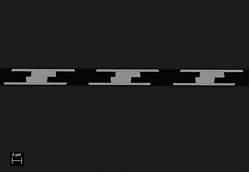
Process development for advanced direct oxide-oxide and Cu-Cu bonding (DBI)

The hybrid bonding technology is jointly developed by XPERI (Invensas) and IZM-ASSID on 300 mm wafer size. The DBI is an extension of Ziptronix‘ ZiBond® technology that allows an interconnect pitch of very few micrometers and accommodates 1.5 million connections per cm². ZiBond® is a low temperature homogeneous (e. g. oxide-to-oxide) direct bonding technology that forms strong bonds between wafers or dies with same or different coefficients of thermal expansion (CTE). The process uses leading-edge process tools and advanced CMP materials to achieve state of the art planarization performance. The electrical connection by bonding of 300 mm wafers was established by using a IZM-ASSID test chip design: 2 half chips with two neighboring daisy chains each and 6,656 interconnects per chain. A yield of > 95 percent could be demonstrated. The benefits of the DBI are: fine pitch 3D interconnect (scales from <10 μm to 1 μm or less), high bandwidth (enables increase in I/O as needed), improved performance (enhanced electrical and thermal characteristics due to elimination of micro bumps, underfill and solder), yield improvement (minimized warpage during assembly) as well as low cost (reduced process steps and simplified manufacturing process).

© Fraunhofer IZM-ASSID
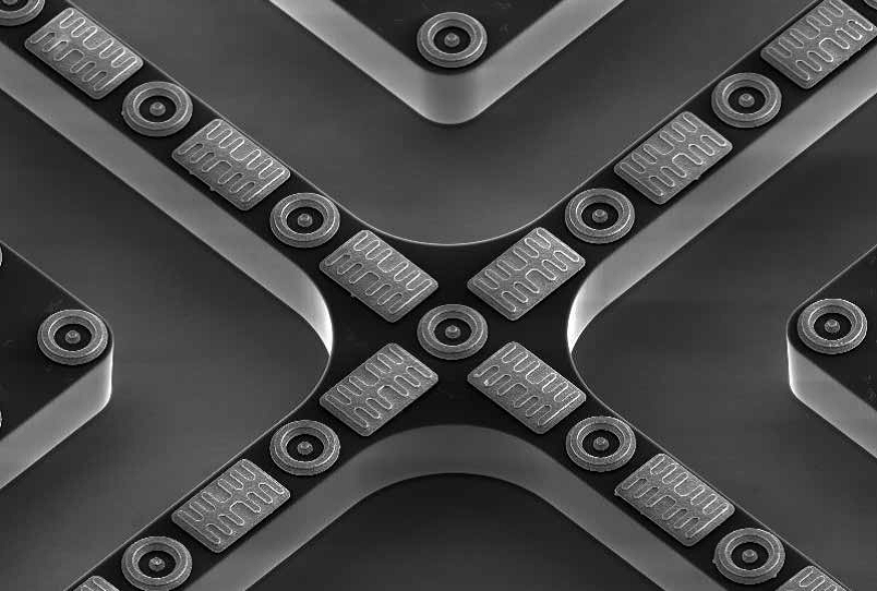
REM-Aufnahme einer Interposerhälfte mit Gräben im Silizium, die nach dem Bonden beider Hälften einen Mikrokanal für die Flüssigkühlung bilden.

Interposer with micro-fluidic-cooling

The maximum processor performance is limited by the heat removal efficiency. Therefore, a highly effective cooling technology as well as an innovative power management are the keys to increase the computing power. While air cooling is limited, a liquid cooling approach can meet these high requirements by targeting at a double-sided processor cooling. Within the project CarrICool, IZM-ASSID worked on the realization of a double-sided liquid cooling technology by innovatively integrating horizontal and vertical microfluidic channels. These micro channels are integrated in an electrically full functional interposer stack with Cu-TSVs in a waterproof manner. With this, for the first time, high performance processors can be additionally and effectively cooled from the bottom side, too. In combination with the integrated cooling plate on the top side of the processor, this double-sided cooling configuration allows the dissipation of 672 W heat from a 4 cm² sized processor surface with a maximum coolant temperature increase of only 60 °C. Compared to the performance of a common kitchen hotplate, this equals a forty times higher heating power when considering the same area size.