 Fraunhofer Dresden
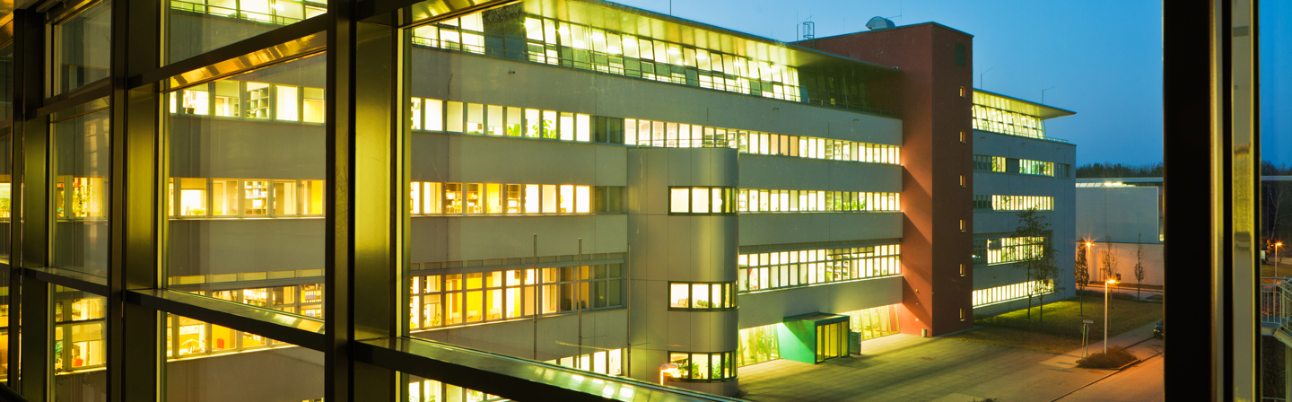
Brief Profile
Fraunhofer IPMS stands for applied research and development at the highest international level in the fields of photonic microsystems, microsystem technologies, nanoelectronic technologies and wireless microsystems. Innovative processes and products using our technologies can be found in all major markets - such as information and communication technologies, consumer goods, automotive technology, semiconductors, measurement and medical technology.
The headquarters are located at Maria-Reiche-Straße 2 in Dresden-Klotzsche. A MOEMS/MEMS cleanroom of 1500 m² (class 4 according to ISO 14644-1) can be found at the premises, which can be used for technology development up to pilot production of innovative microsystems on 200 mm. The range of services includes wafer processing, characterization & test, packaging and interconnection technology as well as the organization of external services and subcontracting.
The "Center Nanoelectronic Technologies" division has its own cleanroom infrastructure for process and material development on 300 mm wafers with its location"An der Bartlake 5" in the immediate vicinity of the chip manufacturer Globalfoundries. For processing customer orders, 4000 m² of clean room space of class 6 and 3 (according to ISO 14644-1) as well as laboratory space for more than 60 processing and analytical tools are available. The equipment park includes deposition and etching equipment as well as inspection and analysis equipment for determining defects and measuring coating properties.
At our Cottbus site, we work on monolithic integrated actuator and sensor systems as well as terahertz micromodules and applications in the "Integrated Silicon Systems" branch of the institute.
In the Fraunhofer Center for "Microelectronic and Optical Systems for Biomedicine", operated jointly with Fraunhofer IOF and IZI in Erfurt, the focus is on novel systems for applications in biomedicine.
To meet the expectations of our customers, our company is certified by DEKRA according to the DIN EN 9001:2015 standard for research, development and manufacturing, the corresponding semiconductor and microsystem processes, integrated actuator/sensor technology and consulting.