Research highlights from Fraunhofer IPMS

© 2013 Sven Döring / Agentur Focus
Waferabbildung eines eindimensionalen Flächenlichtmodulators.

Spatial Light Modulators

The spatial light modulators developed at Fraunhofer IPMS consist of arrays of micromirrors on semiconductor chips, whereby the number of mirrors varies depending on the application, from a few hundred to several millions. In most cases this requires a highly integrated application-specific electronic circuit (ASIC) as basis for the component architecture in order to enable an individual analog deflection of each micromirror. In addition, Fraunhofer IPMS develops electronics and software for mirror array control.

The individual mirrors that vary in number and size per chip can be tilted or vertically deflected depending on the application, so that a surface pattern is created, for example to project defined structures. High-resolution tilting mirror arrays with up to 2.2 million individual mirrors are used by our customers as highly dynamic programmable masks for optical micro-lithography in the ultraviolet spectral range. The mirror dimensions are 10 μm or larger. By tilting the micromirrors, structural information is transferred to a high-resolution photo resist at high frame rates. Further fields of application are mask inspection and measurement technology for the semiconductor industry, microscopy and prospectively laser printing, marking and material processing.

Piston micromirror arrays can for example be used for wavefront control in adaptive optical systems. These systems can correct wavefront disturbances in broad spectral ranges and thereby improve image quality. The component capabilities attract special interest in the fields of ophthalmology, astronomy and microscopy, as well as in spatial and temporal laser beam and pulse shaping.

© 2013 Sven Döring / Agentur Focus
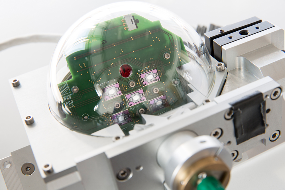
Optischer Scankopf einer 3D-TOF-Kamera mit integriertem MEMS Scannerspiegel-Array des Fraunhofer IPMS.
© Fraunhofer IPMS
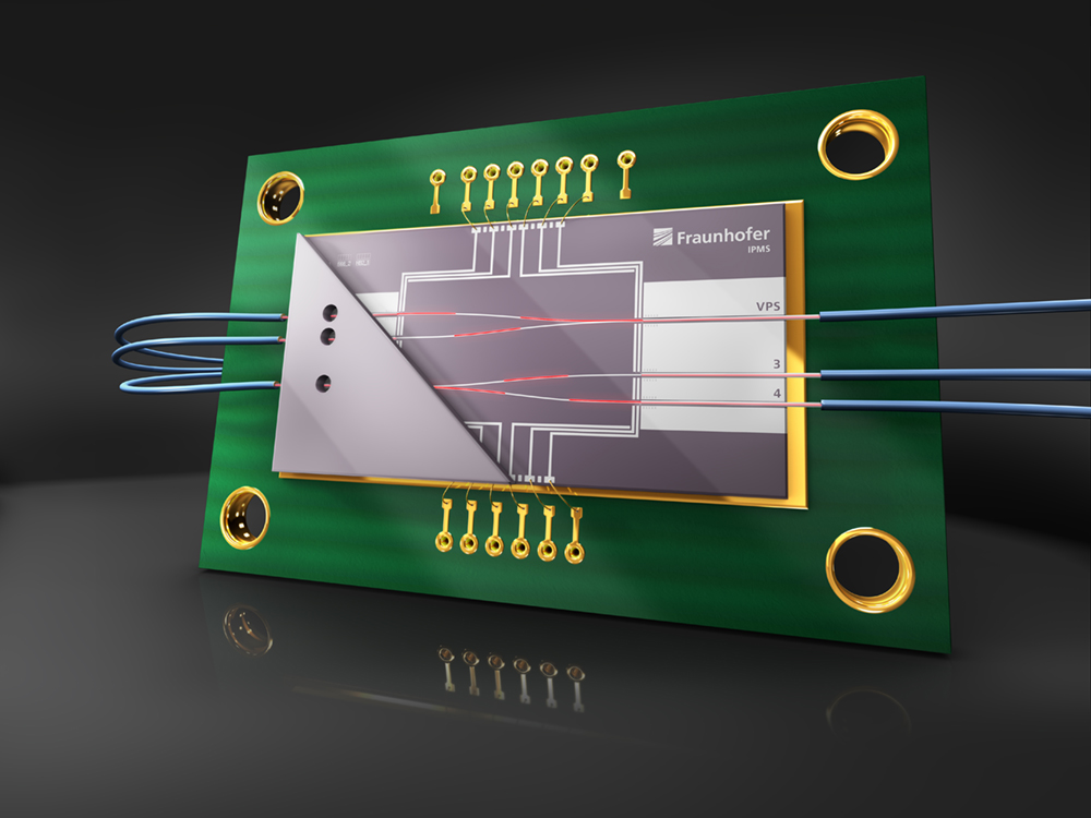
Flüssigkristall-Wellenleiter.

MEMS Scanners

To date, more than 50 different resonant scanners have been designed and manufactured. They are made to deflect light either one-dimensionally or two-dimensionally or for high-speed optical path length modulation. Scan frequencies from 0.1 kHz to 50 kHz have been successfully executed. Applications range from reading barcode and data code, through 3D metrology, and right up to laser projection and spectroscopy. An example is a MEMS scanner with integrated diffraction grating for spectroscopic applications which HiperScan GmbH, a Fraunhofer IPMS spin-off, has been distributing since 2007 a novel infrared wavelength micro spectrometer. Furthermore, the Fraunhofer IPMS is engaged in custom-designed scanning mirrors, e.g. for Fourier Transform spectrometers, confocal microscopy, highly miniaturized displays, ultra-compact laser projection systems, endoscopic image acquisition as well as triangulation.

In addition to resonant scanners, quasi-static micro-scanners are also under development. These activities are geared toward applications such as laser beam positioning and switching.

The internet platform www.micro-mirrors.com was introduced, allowing customers to define and order resonant micro-scanners that are suitable for their specific applications. Thanks to a building-block approach, we are able to offer reasonably-priced devices with a short lead time.

© Fraunhofer IPMS
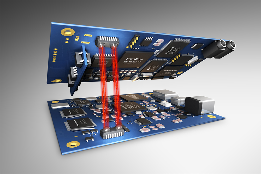
Mit der Li-Fi-GigaDock-Technologie können kurze Kabel und Steckverbinder bei Datenraten von bis zu 12,5 GBit/s ersetzt werden.

Wireless Microsystems

The business unit “Wireless Microsystems” provides product-related partial and complete solutions for customer- and application-specific problems of hard- and software. This includes optical wire­less communication (Li-Fi), maintenance-free and battery-free RFID sensor nodes, integrated intercon­nected systems, track and trace as well as big data and data analysis. Technological priorities lie in the development of components and modules for RFID and Li-Fi. Supported technology nodes for passive transponders are LF, HF, NFC and UHF. The focus is on antenna design, custom RF ASICs, sensor integration and interconnected RFID platforms via OPC UA. The developments of Li-Fi technology are divided into docking and hot spot solutions for data rates of a few kilobits per second up to the current maximum transmission rate of 12.5 Gbps. The aim is to replace plugs, cables and wireless technologies by perfor­mant, real-time optical wireless communication in various applications. Development focuses on optics, analog front ends, specific protocols and protocol adapters to easily connect Li-Fi solutions to existing infrastructure.

OPC UA coupled RFID sensor networks and real time location services in buildings provide the basis to develop user-specific value-added services. These services include indoor navigation, location-based services, locating assets in manufacturing, electronic lot traveller and production optimization, workforce management, preventive maintenance of equipment and much more.

© Fraunhofer IPMS
Hyperspektralen Bildgebung am Beispiel eines Apfels.

Environmental Sensing

The “Environmental Sensing” (ENV) business unit focuses on the development of sensory de­vices, components and subsystems to be used in application-specific devices for the detection and evaluation of environmental conditions. For this purpose, Fraunhofer IPMS develops silicon-based microsystems technology components such as solid-state sensors, ultrasonic transducers as well as photonic sensors and modulators. These sensory elements are fully-developed over functional models, prototypes and pre-series to ultimately be used in systems designed and implemented in the business unit. The wide range of application areas includes food monitoring, water and soil analysis, industrial metrology, security and medical technology. In ad­dition, Fraunhofer IPMS can provide feasibility stud­ies, test measurements and the characterization of sensory elements and systems.

Know-how specific to the business unit includes comprehensive knowledge for the production of MEMS components and characterization as well as performance and operating-point determination for each application. Highly precise, state-of-the-art micro-mounting equipment that allows accurate placement of devices in the single-digit micrometer range as well as spectral characterization tools (e.g., various spectrometer types NIR to FTIR, spectro­graphs, monochromator with integrating sphere, FFT analyzer) are utilized. Upon this foundation, it is, for example, possible to construct state-of-the-art minia­ture optical spectrometers in the size of a sugar cube.

© Fraunhofer IPMS

Neuromorphic Computing

Increasing digitization is constantly driving the demands on electronic hardware. Speed, performance, miniaturization and energy efficiency are becoming increasingly important when it comes to enabling Big Data and Artificial Intelligence (AI) applications.

A promising solution approach is offered by so-called neuromorphic computing, which aims to emulate the self-organizing and self-learning nature of the brain. Fraunhofer IPMS develops materials, technologies and complete hardware solutions with high energy efficiency, especially for edge applications.

The technological developments are pursued in different stages of expansion. The so-called "deep neural networks" (DNN) have already arrived in the application with the help of classical technologies (e.g. SRAM or flash-based) and initially emulate the parallelism and efficiency of the brain. Further miniaturization and reduction of power consumption for edge applications is possible using new, innovative technologies. The subsequent generation of so-called "Spiking Neural Networks" (SNN) attempts to additionally physically replicate the temporal component of the functionality of neurons and synapses, which enables even higher energy efficiency and plasticity. Again, innovative technology concepts show promise over classical technologies.

For both generations of neuromorphic hardware, Fraunhofer IPMS is exploring crossbar architectures based on non-volatile memories, the ferroelectric field effect transistors. This is done within various European (TEMPO, ANDANTE, STORAIGE) and Fraunhofer internally funded projects. Particularly innovative materials research for future SNNs using Li-based systems is being conducted within the Saxon project MEMION.


© Fraunhofer IPMS

Quantencomputing

Quantum computers have the potential to exceed the limits of conventional computing systems many times over. Medicine, logistics, material development and cryptography are just some of the fields that can experience enormous progress through quantum computers. Although there are already a variety of different approaches to quantum computing, there are currently only a few realizations in Germany that go beyond the laboratory setup.

Therefore, Fraunhofer IPMS is researching scalable technologies for semiconductor qubits together with German and European partners. For this purpose, we develop industry-oriented CMOS-compatible manufacturing methods. We deal with all important components of quantum computers, from material screening, process development and new integration concepts to characterization and implementation of necessary drive electronics. The state-of-the-art 300 mm semiconductor infrastructure of the Center Nanoelectronic Technologies offers excellent conditions for this.

Our research topics at a glance:

  • Fabrication of qubits and their electronic interfacing, with special emphasis on industry-oriented scalability (Si/ SiGe, Si-MOSFET and superconducting qubit technologies)
  • Development of new and optimized materials, processes and integration concepts for cryoelectronics as well as superconducting metallization concepts
  • Development of manufacturing processes for nanostructuring, but also material development and electrical control from the CMOS area